2024-06-18 ハーバード大学
<関連情報>
- https://seas.harvard.edu/news/2024/06/quantum-world-silicon-chip
- https://www.nature.com/articles/s41467-024-48968-w
シリコン中の電気通信カラーセンターの電気的操作 Electrical manipulation of telecom color centers in silicon
Aaron M. Day,Madison Sutula,Jonathan R. Dietz,Alexander Raun,Denis D. Sukachev,Mihir K. Bhaskar & Evelyn L. Hu
Nature Communications Published:03 June 2024
DOI:https://doi.org/10.1038/s41467-024-48968-w

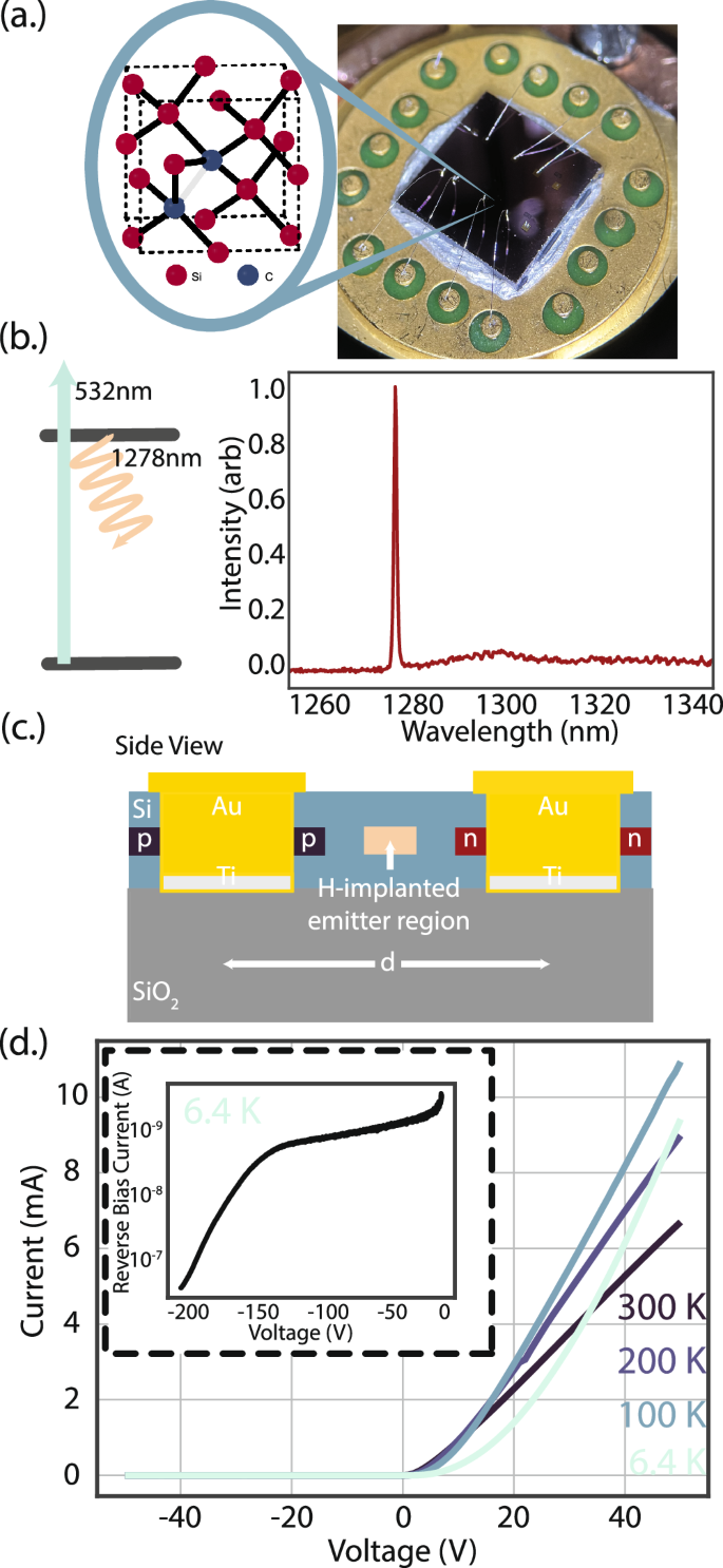
Abstract
Silicon color centers have recently emerged as promising candidates for commercial quantum technology, yet their interaction with electric fields has yet to be investigated. In this paper, we demonstrate electrical manipulation of telecom silicon color centers by implementing novel lateral electrical diodes with an integrated G center ensemble in a commercial silicon on insulator wafer. The ensemble optical response is characterized under application of a reverse-biased DC electric field, observing both 100% modulation of fluorescence signal, and wavelength redshift of approximately 1.24 ± 0.08 GHz/V above a threshold voltage. Finally, we use G center fluorescence to directly image the electric field distribution within the devices, obtaining insight into the spatial and voltage-dependent variation of the junction depletion region and the associated mediating effects on the ensemble. Strong correlation between emitter-field coupling and generated photocurrent is observed. Our demonstration enables electrical control and stabilization of semiconductor quantum emitters.


