走査型トンネル顕微鏡の新手法で、化合物表面での電子の動きを解明 New scanning tunneling microscopy method demystifies what electrons are doing on the surface of a compound.
2023-03-30 ハーバード大学
この方法により、物質が電気を伝導するか絶縁するかを理解する上での画期的な発見が可能になった。化合物の一つであるSamarium Hexaboride (SmB6)の場合、表面を通じて電気を伝導する性質を持つトポロジカル・インシュレーターであることが2019年に明らかになっていたが、表面以外での伝導性については謎が残っていた。
今回の方法により、単一原子レベルでの電荷の分布が明らかになり、SmB6の性質に関する新たな理解が得られた。これにより、今後、世界をより細かく見るための強力な高分解能ツールが得られる可能性がある。
<関連情報>
- https://seas.harvard.edu/news/2023/03/imaging-technique-reveals-electronic-charges-single-atom-resolution
- https://www.science.org/doi/abs/10.1126/science.abq5375
- https://www.nature.com/articles/s41567-019-0700-8
近藤絶縁体における金属的挙動の原子レベルの起源を可視化する Visualizing the atomic-scale origin of metallic behavior in Kondo insulators
Harris Pirie ,Eric Mascot ,Christian E. Matt ,Yu Liu ,Pengcheng Chen ,M. H. Hamidian ,Shanta Saha ,Xiangfeng Wang,Johnpierre Paglione ,Graeme Luke ,David Goldhaber-Gordon ,Cyrus F. Hirjibehedin ,J. C. Séamus Davis ,Dirk K. Morr ,Jennifer E. Hoffman
Science Published:23 Mar 2023
DOI:https://doi.org/10.1126/science.abq5375
Metallic puddles in an insulator
Certain properties of metals can oscillate as a function of applied magnetic fields, a phenomenon known as quantum oscillations. This process should not happen in insulators, which is what made the observation of quantum oscillations in the Kondo insulator samarium hexaboride so surprising. Multiple mechanisms, both intrinsic and extrinsic, have been proposed to explain these findings. Pirie et al. used scanning tunneling microscopy to study the vicinity of defects, including substitutions and vacancies. They found that the defects caused the formation of localized metallic puddles, which could explain the previously observed metal-like properties of this insulator. —JS
Abstract
A Kondo lattice is often electrically insulating at low temperatures. However, several recent experiments have detected signatures of bulk metallicity within this Kondo insulating phase. In this study, we visualized the real-space charge landscape within a Kondo lattice with atomic resolution using a scanning tunneling microscope. We discovered nanometer-scale puddles of metallic conduction electrons centered around uranium-site substitutions in the heavy-fermion compound uranium ruthenium silicide (URu2Si2) and around samarium-site defects in the topological Kondo insulator samarium hexaboride (SmB6). These defects disturbed the Kondo screening cloud, leaving behind a fingerprint of the metallic parent state. Our results suggest that the three-dimensional quantum oscillations measured in SmB6 arise from Kondo-lattice defects, although we cannot exclude other explanations. Our imaging technique could enable the development of atomic-scale charge sensors using heavy-fermion probes.
トポロジカル近藤絶縁体の重いディラック・フェルミオンが出現する様子をとらえる Imaging emergent heavy Dirac fermions of a topological Kondo insulator
Harris Pirie,Yu Liu,Anjan Soumyanarayanan,Pengcheng Chen,Yang He,M. M. Yee,P. F. S. Rosa,J. D. Thompson,Dae-Jeong Kim,Z. Fisk,Xiangfeng Wang,Johnpierre Paglione,Dirk K. Morr,M. H. Hamidian & Jennifer E. Hoffman Published:11 November 2019
DOI:https://doi.org/10.1038/s41567-019-0700-8

Abstract
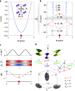
The interplay between strong electron interactions and band topology is a new frontier in the search for exotic quantum phases. The Kondo insulator SmB6 has emerged as a promising platform because its correlation-driven bulk gap is predicted to host topological surface modes entangled with f electrons, spawning heavy Dirac fermions1,2,3,4. Unlike the conventional surface states of non-interacting topological insulators, heavy Dirac fermions are expected to harbour spontaneously generated quantum anomalous Hall states5, non-Abelian quantum statistics6,7, fractionalization8 and topological order6,7,8. However, the small energy scales required to probe heavy Dirac fermions have complicated their experimental realization. Here we use high-energy-resolution spectroscopic imaging in real and momentum space on SmB6. On cooling below 35 K, we observe the opening of an insulating gap that expands to 14 meV at 2 K. Within the gap, we image the formation of linearly dispersing surface states with effective masses reaching 410 ± 20 me (where me is the mass of the electron). Our results demonstrate the presence of correlation-driven heavy surface states in SmB6, in agreement with theoretical predictions1,2,3,4. Their high effective mass translates to a large density of states near zero energy, which magnifies their susceptibility to the anticipated novel orders and their potential utility.


