2025-12-17 中国科学院(CAS)

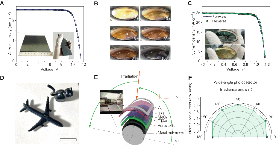
Applications of perovskite films fabricated by spray coating. (Image by QIBEBT)
<関連情報>
- https://english.cas.cn/newsroom/research_news/chem/202512/t20251216_1137165.shtml
- https://www.cell.com/joule/abstract/S2542-4351(25)00409-X
先進的な太陽光発電向け高品質ペロブスカイト膜を可能にする閉じ込め結晶化戦略 Confined crystallization strategy enabling high-quality perovskite film for advanced photovoltaics
Xiaopeng Feng ∙ Fuzong Xu ∙ Cheng Peng ∙ … ∙ Stefaan De Wolf ∙ Bo Tang ∙ Guanglei Cui
Joule Published:December 16, 2025
DOI:https://doi.org/10.1016/j.joule.2025.102228
Context & scale
Semiconductor devices fabricated on non-developable curved surfaces (with non-zero Gaussian curvature) cannot be adequately realized using flexible substrates alone, as they are limited by local stress, irreversible deformation, poor substrate conformity, and interfacial mismatch. To achieve conformal deposition on such curved surfaces, solution-based spray coating has been recognized as a rapid and cost-effective approach. In recent years, halide perovskites have been intensively studied as emerging optoelectronic semiconductors, leading to remarkable progress in their photovoltaic and photodetection applications. However, the spray deposition of perovskite films has been restricted by uncontrollable crystallization dynamics and environmental humidity, which hinder the formation of high-quality, low-defect films, compared with spin, blade, or slot-die coating.
A solvation regulation strategy was developed, in which the perovskite crystallization process is confined within localized solvent clusters during spray deposition. Through this confined crystallization, the activation energy for precursor-to-crystal conversion is greatly reduced, and the film quality is markedly enhanced. During the solution-based spray deposition process, perovskite can rapidly grow epitaxially along the direction perpendicular to the substrate, thereby enabling the deposition of films with arbitrary thickness. Consequently, high-performance perovskite thin films with tunable thickness, as well as corresponding optoelectronic devices, can be fabricated on arbitrary curved surfaces even under harsh environmental conditions.
Highlights
- Localized solvation enables uniform nucleation, oriented growth, and low-defect films
- Spray-coated perovskite cell reached 25.5% PCE (25.2% certified); module > 22.5%
- Perovskite films deposited at ∼80% R.H. show humidity-tolerant fabrication
- Curved rigid-surface solar cells made without spin coating; PCE > 23.2%
Summary
Spray coating offers great potential for optoelectronic devices with complex geometries, but uniform crystallization remains challenging because of limited control over the process. Herein, we present a localized high-concentration (LHC) precursor strategy that enables homogeneous and confined bulk-phase pre-nucleation within droplets during spraying, effectively addressing spatiotemporal inconsistencies in nucleation. The LHC approach employs weak ligand solvents to restrict the diffusion of A-site cations while enhancing their interaction with [PbIx]2−x complexes, thereby suppressing the formation of solvated intermediate phases and achieving direct α-phase perovskite with high crystallographic orientation and low defect-state density (∼1014 cm−3). This work also established a correlation between solvent-related parameters and device performance, using machine learning. The spray-coated devices achieved power conversion efficiencies (PCEs) of 25.5% (0.09 cm2 small cells), 22.5% (14 cm2 mini-modules), and 23.2% (curved cells). The strategy has been proven to have versatile applications, including in high-humidity environments (relative humidity [(R.H.] ∼80%, 23.1%), complex surfaces, and mask-assisted patterning.


