2024-07-29 シンガポール国立大学(NUS)
<関連情報>
- https://news.nus.edu.sg/nus-researchers-develop-technique-to-fabricate-three-dimensional-circuits/
- https://www.nature.com/articles/s41928-024-01207-y
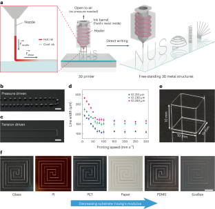
張力駆動による自立フィールドの金属構造の三次元印刷 Tension-driven three-dimensional printing of free-standing Field’s metal structures
Shaohua Ling,Xi Tian,Qihang Zeng,Zhihang Qin,Selman A. Kurt,Yu Jun Tan,Jerry Y. H. Fuh,Zhuangjian Liu,Michael D. Dickey,John S. Ho & Benjamin C. K. Tee
Nature Electronics Published:25 July 2024
DOI:https://doi.org/10.1038/s41928-024-01207-y

Abstract
The direct writing of complex three-dimensional (3D) metallic structures is of use in the development of advanced electronics. However, conventional direct ink writing primarily uses composite inks that have low electrical conductivity and require support materials to create 3D architectures. Here we show that Field’s metal—a eutectic alloy with a relatively low melting point—can be 3D printed using a process in which tension between the molten metal in a nozzle and the leading edge of the printed part allows 3D structures to be directly written. The use of tension avoids using external pressure for extrusion (which can cause beading of the printed structure), allowing uniform and smooth microwire structures to be printed on various substrates with speeds of up to 100 mm s−1. We use the approach to print various free-standing 3D structures—including vertical letters, a cubic framework and scalable helixes—without post-treatment, and the resulting Field’s metal structures can offer electrical conductivity of 2 × 10⁴ S cm−1, self-healing capability and recyclability. We also use the technique to print a 3D circuit for wearable battery-free temperature sensing, hemispherical helical antennas for wireless vital sign monitoring and 3D metamaterials for electromagnetic-wave manipulation.


