2026-02-19 スイス連邦工科大学ローザンヌ校(EPFL)

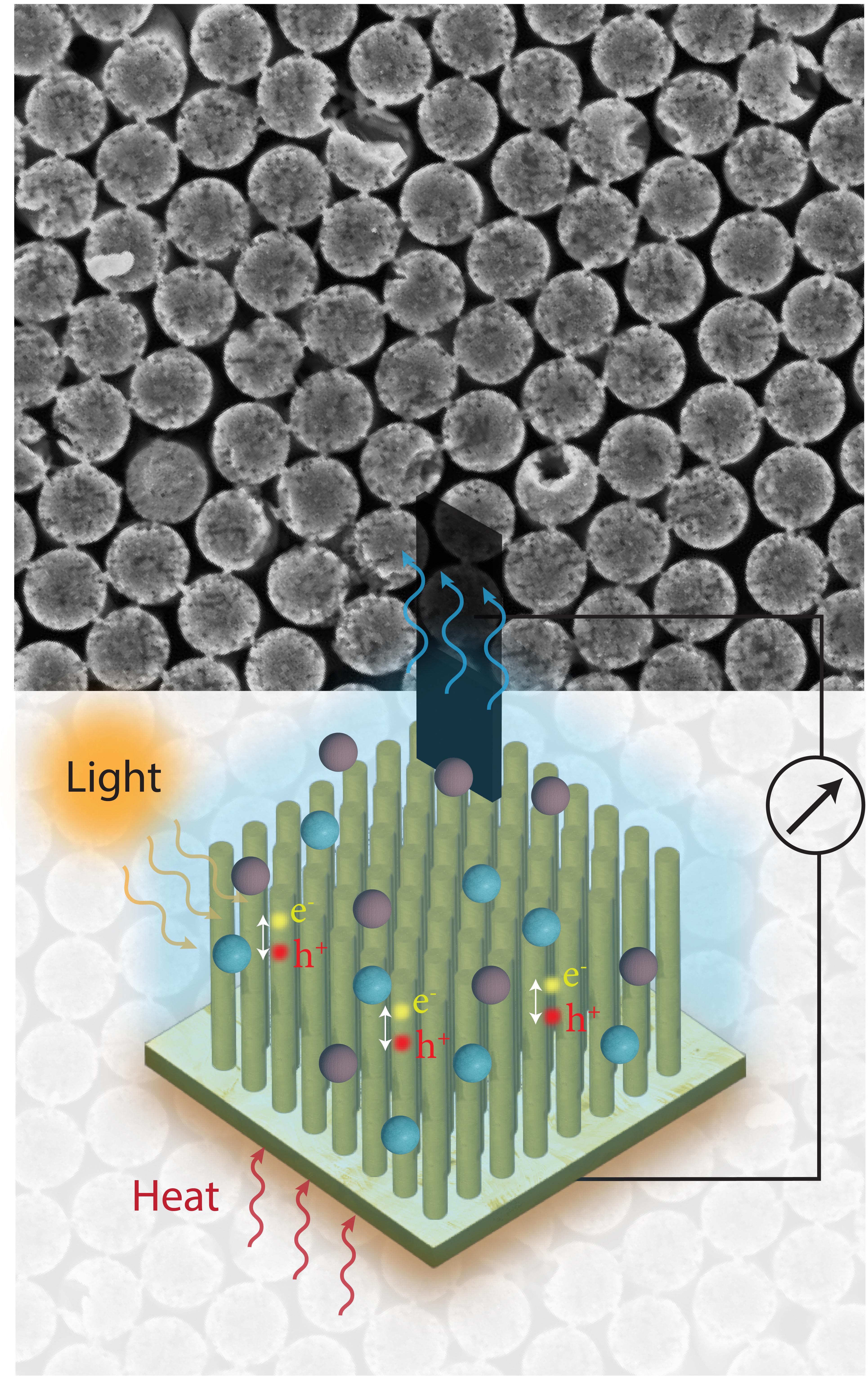
Schematic of the hydrovoltaic device with a top evaporating electrode surface and a bottom
array of silicon nanopillars immersed in water. 2026 LNET EPFL CC BY SA
<関連情報>
- https://actu.epfl.ch/news/nanodevice-produces-continuous-electricity-from–2/
- https://www.nature.com/articles/s41467-025-68261-8
熱と光駆動による表面電荷ダイナミクスの結合による水力発電の強化 Enhancing hydrovoltaic power generation through coupled heat and light-driven surface charge dynamics
Tarique Anwar & Giulia Tagliabue
Nature Communications Published:09 January 2026
DOI:https://doi.org/10.1038/s41467-025-68261-8
Abstract
Harnessing natural evaporation offers a sustainable pathway for next-generation energy technologies. We present a unified physical and experimental framework for evaporation-driven hydrovoltaic (EDHV) systems that decouples and controls the key interfacial processes underlying electricity generation from heat and sunlight. An intermediate ion-conducting layer separates the evaporative top interface from the silicon–dielectric nanopillar array, enabling independent modulation of evaporation, ion transport, and interfacial chemical equilibrium. This strategy enhances performance and clarifies mechanisms governing thermal and photo-induced charge generation, improving ion migration and electricity output. We develop a predictive equivalent-circuit model that captures process coupling through an analytically derived transfer capacitance. Our results show that capacitive photocharging and thermally modulated surface equilibria—rather than faradaic or photothermal effects—dominate energy conversion. The device achieves 1 V open-circuit voltage and 0.25 W/m² power density, with silicon doping and dielectric choice further boosting performance. These findings inform EDHV optimization across environmental and material conditions.


