2026-01-05 ペンシルベニア州立大学(Penn State)

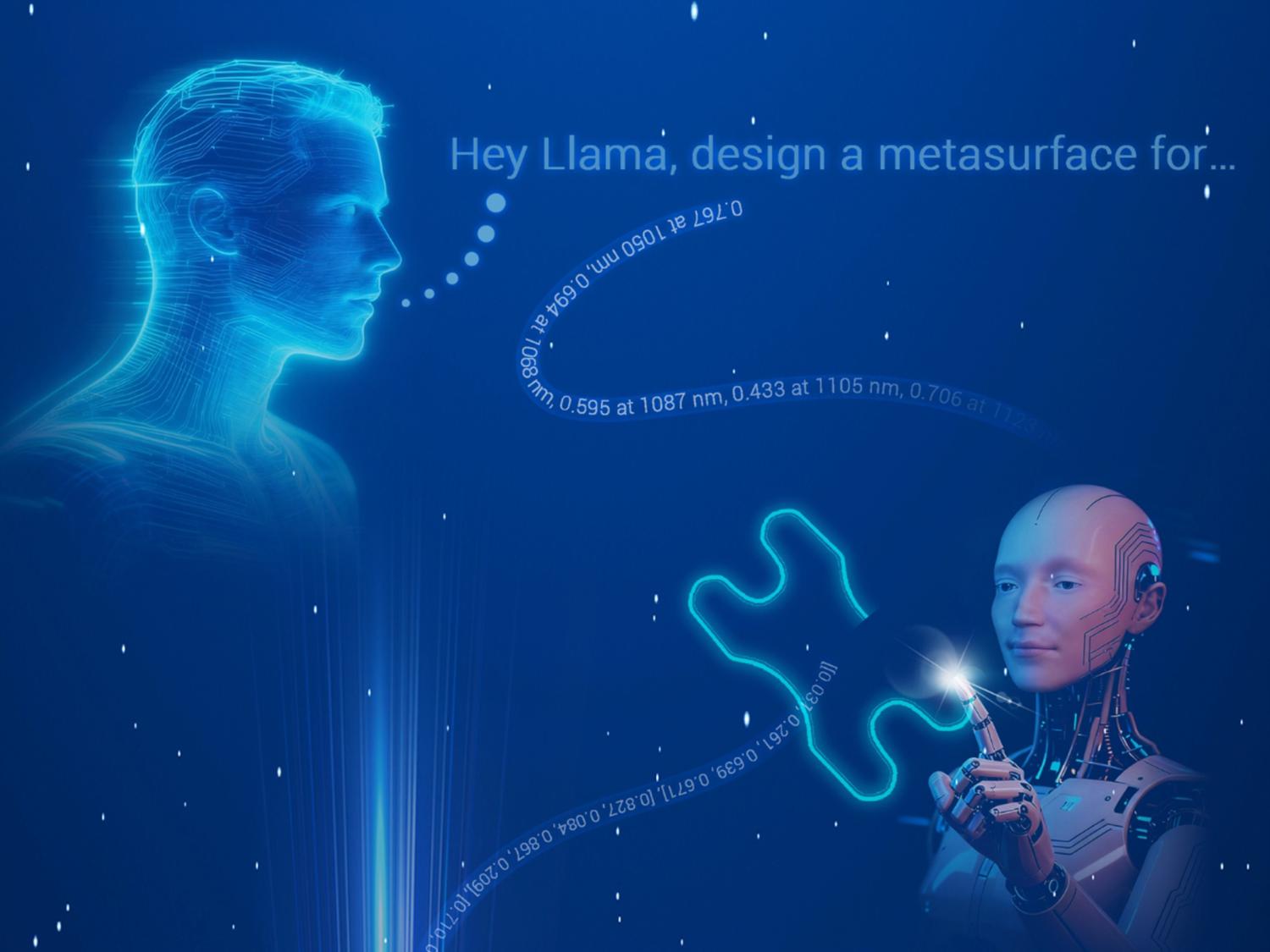
A group of researchers at Penn State developed an approach that integrates artificial intelligence into metasurface design. Their work was featured on the cover of the October issue of Nanophotonics. Credit: Provided by Huanshu Zhang. All Rights Reserved.
<関連情報>
- https://www.psu.edu/news/engineering/story/ai-approach-takes-optical-system-design-months-milliseconds
- https://www.degruyterbrill.com/document/doi/10.1515/nanoph-2025-0343/html
チャットからチップへ:大規模言語モデルに基づく任意形状メタサーフェスの設計 Chat to chip: large language model based design of arbitrarily shaped metasurfaces
Huanshu Zhang, Lei Kang, Sawyer D. Campbell and Douglas H. Werner
Nanophotonics Published:October 9, 2025
DOI:https://doi.org/10.1515/nanoph-2025-0343
Abstract
Traditional metasurface design is limited by the computational cost of full-wave simulations, preventing thorough exploration of complex configurations. Data-driven approaches have emerged as a solution to this bottleneck, replacing costly simulations with rapid neural network evaluations and enabling near-instant design for meta-atoms. Despite advances, implementing a new optical function still requires building and training a task-specific network, along with exhaustive searches for suitable architectures and hyperparameters. Pre-trained large language models (LLMs), by contrast, sidestep this laborious process with a simple fine-tuning technique. However, applying LLMs to the design of nanophotonic devices, particularly for arbitrarily shaped metasurfaces, is still in its early stages; as such tasks often require graphical networks. Here, we show that an LLM, fed with descriptive inputs of arbitrarily shaped metasurface geometries, can learn the physical relationships needed for spectral prediction and inverse design. We further benchmarked a range of open-weight LLMs and identified relationships between accuracy and model size at the billion-parameter level. We demonstrated that 1-D token-wise LLMs provide a practical tool for designing 2-D arbitrarily shaped metasurfaces. Linking natural-language interaction to electromagnetic modelling, this “chat-to-chip” workflow represents a step toward more user-friendly data-driven nanophotonics.


