2025-04-16 京都大学
<関連情報>
- https://www.kyoto-u.ac.jp/ja/research-news/2025-04-16
- https://www.kyoto-u.ac.jp/sites/default/files/2025-04/web_2504_Nishikawa-9d89fd2d8897b4e49f471f013eaaea78.pdf
- https://www.nature.com/articles/s41467-025-58629-1
室温での炭化ケイ素中の単一スピンのコヒーレント光電気読み出し Coherent photoelectrical readout of single spins in silicon carbide at room temperature
Tetsuri Nishikawa,Naoya Morioka,Hiroshi Abe,Koichi Murata,Kazuki Okajima,Takeshi Ohshima,Hidekazu Tsuchida & Norikazu Mizuochi
Nature Communications Published:15 April 2025
DOI:https://doi.org/10.1038/s41467-025-58629-1

Abstract
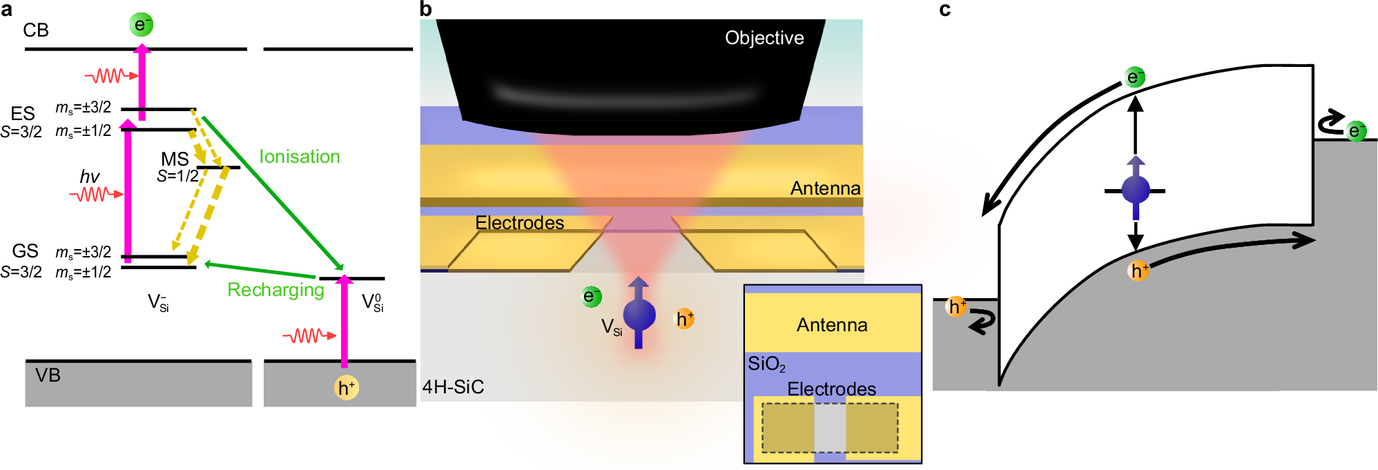
Establishing a robust and integratable quantum system capable of sensitive qubit readout at ambient conditions is a key challenge for developing prevalent quantum technologies, including quantum networks and quantum sensing. Paramagnetic colour centres in wide bandgap semiconductors provide optical single-spin detection, yet realising efficient electrical readout technology in scalable material will unchain developing integrated ambient quantum electronics. Here, we demonstrate photoelectrical detection of single spins in silicon carbide, a material amenable to large-scale processing and electronic integration. With efficient photocarrier collection, we achieve a 1.7–2 times better signal-to-noise ratio for single spins of silicon vacancies with electrical detection than with optical detection suffering from saturating fluorescence and internal reflection. Based on our photoionisation dynamics study, further improvement would be expected with enhanced ionisation. We also observe single-defect-like features in the photocurrent image where photoluminescence is absent in the spectrum range of silicon vacancies. The efficient electrical readout in the mature material platform holds promise for developing integrated quantum devices.


