2024-08-20 パデュー大学
<関連情報>
- https://www.purdue.edu/newsroom/2024/Q3/inspired-by-the-human-body-engineer-designs-chips-that-could-make-wearable-ai-more-energy-efficient/
- https://arxiv.org/abs/2406.18791
- https://medibio.tiisys.com/119774/#google_vignette
- https://ieeexplore.ieee.org/document/9743554
- https://medibio.tiisys.com/
- https://ieeexplore.ieee.org/document/8805102
招待: 人間に着想を得た分散型ウェアラブルAI Invited: Human-Inspired Distributed Wearable AI
Shreyas Sen, Arunashish Datta
arXiv last revised 12 Jul 2024 (this version, v2)
DOI:https://doi.org/10.48550/arXiv.2406.18791

Abstract
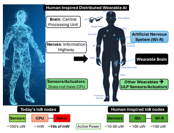
The explosive surge in Human-AI interactions, fused with a soaring fascination in wearable technology, has ignited a frenzy of innovation and the emergence of a myriad of Wearable AI devices, each wielding diverse form factors, tackling tasks from health surveillance to turbocharging productivity. This paper delves into the vision for wearable AI technology, addressing the technical bottlenecks that stand in the way of its promised advancements.
Embracing a paradigm shift, we introduce a Human-Inspired Distributed Network for Wearable AI, enabled by high-speed ultra-low-power secure connectivity via the emerging ‘Body as a Wire’ (Wi-R) technology. This breakthrough acts as the missing link: the artificial nervous system, seamlessly interconnecting all wearables and implantables, ushering in a new era of interconnected intelligence, where featherweight, perpetually operating wearable AI nodes redefine the boundaries of possibility.
アクター・クリティカル・ニューロコントローラーによるオンチップDNN最適化とリアルタイム計算・通信トレードオフをサポートする65nmワイヤレス画像SoC A 65 nm Wireless Image SoC Supporting On-Chip DNN Optimization and Real-Time Computation-Communication Trade-Off via Actor-Critical Neuro-Controller
Ningyuan Cao; Baibhab Chatterjee; Jianbo Liu; Boyang …
IEEE Journal of Solid-State Circuits Published:28 March 2022
DOI:https://doi.org/10.1109/JSSC.2022.3159473
Abstract
The widespread proliferation of smart sensors has led to hardware that enable edge intelligence (EI) with extreme energy efficiencies. This decreases the volume of data that is transmitted to the cloud, thus reducing: 1) processing latency; 2) communication energy; and 3) network congestion. However, this comes with an added cost of computation at the edge node. The cost (energy/latency) of edge computation and the cost of communication to the cloud vary widely depending on operating conditions, which include: 1) information content in the data; 2) algorithm selection; 3) channel conditions (noise, path-loss, etc.); 4) network size, available bandwidth; and 5) resources at the cloud. This article presents a 65 nm wireless image processing SoC for real-time computation-communication trade-off on resource-constrained edge devices. The test-chip includes: 1) an all-digital, near-memory, reconfigurable, and programmable neural-network (NN)-based systolic image processor; 2) a digitally adaptive radio-frequency digital-to-analog converter (RF-DAC)-based transceiver; and 3) a mixed-signal, time-based, actor-critic (AC) neuro-controller with compute-in-memory (CIM) and in-place weight updates that provide online learning and adaptation for efficiently controlling the computation, communication blocks separately as well as jointly. The major contributions of the proposed SoC are threefold: 1) a wireless Internet of Things (IoT) SoC architecture enabling a generic computation-communication trade-off scheme; 2) a novel CIM circuit design enabling effective AC control and online learning (0.59 pJ/MAC, 0.4 pJ/update); 3) integration of programmable deep NN (DNN) accelerator (1.05 TOPS/W) and reconfigurable transceiver (184 pJ/b @ –15 dBm) supporting versatile cloud-edge collaborations; and 4) significant system-level energy efficiency improvement (5.7 $\times $ ) with real-time on-chip smart control enabled by seamless chip integration and AI-enabled decision-making. Furthermore, this SoC serves as a system-level IoT prototype for next-generation context-aware EI.
身体装着型ビデオセンシングARノード用のスイッチトキャパシタ断熱シグナリングとコンビナトリアルパルス位置変調を備えた65nm 63.3µW 15Mbpsトランシーバ A 65nm 63.3µW 15Mbps Transceiver with Switched-Capacitor Adiabatic Signaling and Combinatorial-Pulse-Position Modulation for Body-Worn Video-Sensing AR Nodes
Baibhab Chatterjee; Arunashish Datta; Mayukh Nath; Ga …
2022 IEEE International Solid-State Circuits Conference Published:17 March 2022
DOI:https://doi.org/10.1109/ISSCC42614.2022.9731793
Abstract
Recent advances in audio-visual augmented reality (AR) and virtual reality (VR) demands 1) high speed (>10Mbps) data transfer among wearable devices around the human body with 2) low transceiver (TRX) power consumption for longer lifetime, especially as communication energy/b is often orders of magnitude higher than computation energy/switching. While WiFi can transmit compressed video (HD 30fps, compressed @6-12Mbps), it consumes 50-to-400mW power. Bluetooth, on the other hand, is not designed for video transfer. New mm-Wave links can support the required bandwidth but do not support ultra-low-power (<1mW). In recent years, Human-Body Communication (HBC) [1]–[6] has emerged as a promising low-power alternative to traditional wireless communication. However, previous implementations of HBC transmitters (Tx) suffer from a large plate-to-plate capacitance (C p , between signal electrode and local ground of the transmitter) which results in a power consumption of aC p V2f (Fig. 16.6.1) in voltage-mode (VM) HBC. The recently proposed Resonant HBC [6] tries to overcome this problem by resonating C p with a parallel inductor (L). However, the operating frequency is usually < a few 10’s of MHz for low-power Electro-Quasistatic (EQS) operation, resulting in a large/bulky inductor. Moreover, the resonant LC p circuit has a large settling time (≈5Q 2 RC P , where R is the effective series resistance of the inductor) for EQS frequencies which will limit the maximum symbol rate to <1MSps for a 21MHz carrier (the IEEE 802.15.6 standard for HBC), making resonant HBC infeasible for> 10Mb/s applications.
ボディワイヤー 時間領域干渉除去を用いた6.3pJ/b 30Mb/s -30dB SIR耐性の広帯域干渉ロバスト人体通信トランシーバBodyWire: A 6.3-pJ/b 30-Mb/s -30-dB SIR-Tolerant Broadband Interference-Robust Human Body Communication Transceiver Using Time Domain Interference Rejection
Shovan Maity; Baibhab Chatterjee; Gregory Chang,…
IEEE Journal of Solid-State Circuits Published:19 August 2019
DOI:https://doi.org/10.1109/JSSC.2019.2932852
Abstract
Human body communication (HBC) utilizes the human body as the communication medium between devices in and around the body, providing an energy-efficient, secure alternative to radio wave communication traditionally used in body area networks (BAN). However, the human antenna effect results in the human body picking up environmental interference affecting HBC transmissions. Most state-of-the-art HBC transceivers utilize narrowband modulation techniques to communicate using frequencies, which are not affected by interference. In this article, we use capacitive termination and voltage mode communication techniques to utilize the human body as a broadband (BB) communication channel enabling as a BB HBC. An integrating dual data rate (I-DDR) receiver utilizing time-domain interference rejection (TD-IR) through integration and periodic sampling is used for interference-robust BB HBC operation. The proposed receiver can achieve higher energy efficiency as it utilizes the full bandwidth of the body for data transmission and does not require any modulation/demodulation. The BB HBC transceiver is fabricated in the TSMC 65-nm technology. Measurement results show 6.3-pJ/bit energy efficiency at a data rate of 30 Mb/s with -30-dB signal-to-interference ratio (SIR) tolerance, making it 18× energy efficient compared with state-of-the-art HBC transceivers.


