2024-09-20 ペンシルベニア州立大学(PennState)
<関連情報>
- https://www.psu.edu/news/materials-research-institute/story/water-free-manufacturing-approach-could-help-advance-2d
- https://www.nature.com/articles/s41467-024-48429-4
アモルファス窒化ホウ素を高性能2次元エレクトロニクスのために調整する Tailoring amorphous boron nitride for high-performance two-dimensional electronics
Cindy Y. Chen,Zheng Sun,Riccardo Torsi,Ke Wang,Jessica Kachian,Bangzhi Liu,Gilbert B. Rayner Jr,Zhihong Chen,Joerg Appenzeller,Yu-Chuan Lin & Joshua A. Robinson
Nature Communications Published:13 May 2024
DOI:https://doi.org/10.1038/s41467-024-48429-4

Abstract
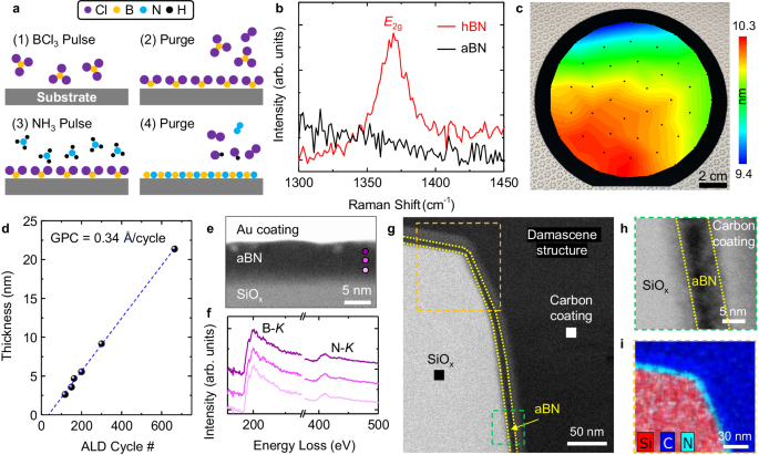
Two-dimensional (2D) materials have garnered significant attention in recent years due to their atomically thin structure and unique electronic and optoelectronic properties. To harness their full potential for applications in next-generation electronics and photonics, precise control over the dielectric environment surrounding the 2D material is critical. The lack of nucleation sites on 2D surfaces to form thin, uniform dielectric layers often leads to interfacial defects that degrade the device performance, posing a major roadblock in the realization of 2D-based devices. Here, we demonstrate a wafer-scale, low-temperature process (<250 °C) using atomic layer deposition (ALD) for the synthesis of uniform, conformal amorphous boron nitride (aBN) thin films. ALD deposition temperatures between 125 and 250 °C result in stoichiometric films with high oxidative stability, yielding a dielectric strength of 8.2 MV/cm. Utilizing a seed-free ALD approach, we form uniform aBN dielectric layers on 2D surfaces and fabricate multiple quantum well structures of aBN/MoS2 and aBN-encapsulated double-gated monolayer (ML) MoS2 field-effect transistors to evaluate the impact of aBN dielectric environment on MoS2 optoelectronic and electronic properties. Our work in scalable aBN dielectric integration paves a way towards realizing the theoretical performance of 2D materials for next-generation electronics.


