(Silicon chip provides low cost solution to help machines see the world clearly)
2021/2/10 英国・サウサンプトン大学
・ サウサンプトン大学オプトエレクトロニック研究センタ-(ORC)とサンフランシスコを拠点とするPointcloud Inc.が、最先端の機械システムの性能と精度を超えるコンパクトな 3D LiDAR イメージングシステムを開発。
・ 3D LiDAR は、自動運転車、顔認識ソフトウェア、自律型ロボットやドローン等多くのアプリケーションで正確なイメージングとマッピングを提供する。正確なイメージングは機械による物理的な世界のマッピングとインタラクションにおいて不可欠であるが、現行技術のサイズとコストがその商業利用を制限している。
・ シリコンのフォトニクスコンポーネントと CMOS 電子回路を同一のマイクロチップにモノリシックに集積化した新 LiDAR のプロトタイプは、低コストのソリューションとして、ロボティクス、自動ナビゲーションシステム、建築現場の安全性の向上やヘルスケア分野に向けたコンパクトな高性能 3D イメージングカメラの大量生産の可能性を拓く。
・ 集積化によるコストのスケールダウン効果は認識されていたが、必要となる性能が達成されていなかった。今回開発したシリコンフォトニクスシステムは、他のチップベースの LiDAR システムや機械的バージョンに比べて飛躍的に高い精度を提供し、LiDAR の集積システムの実現可能性を示している。
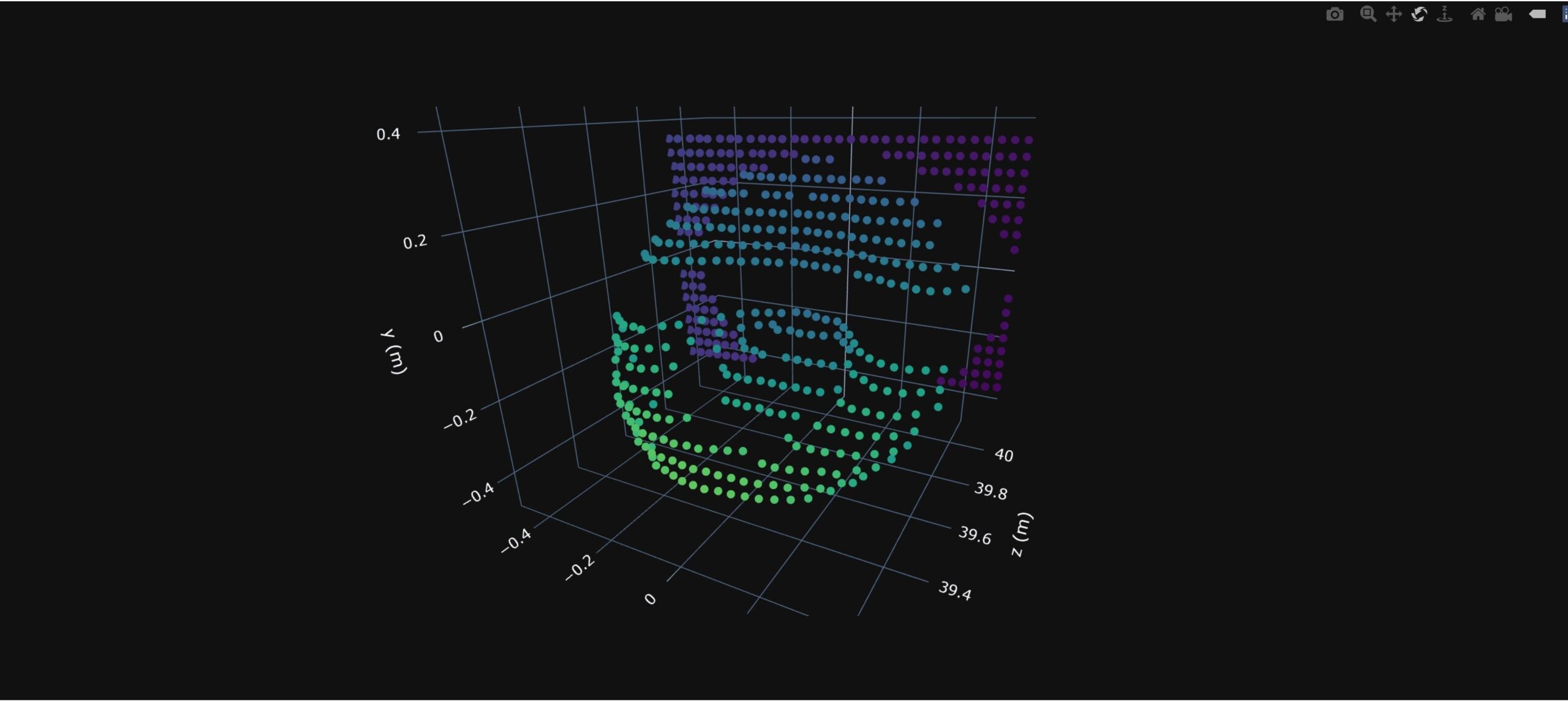
・ 高性能と低コスト製造の組み合わせは、自動化や拡張現実(AR)のアプリケーションを加速させ、産業用・消費者用デジタルツインアプリケーション等の新しい方向性を切り開くもの。新 LiDAR のプロトタイプでは、75m の距離で 3.1mm の精度を達成。
・ 従来の集積システムでは、高密度ピクセルアレイを構成するピクセル数が 20 個以下に制限されていたが、新 LiDAR システムでは、512 個のピクセルから構成される大規模な 2D コヒーレント検出器アレイを初めて実現した。
・ 今後は、同ピクセルアレイとビーム操作技術をさらに進展させることで、新 LiDAR システムを実際のアプリケーションにより適したものにし、性能をさらに向上させる。
URL: https://www.southampton.ac.uk/news/2021/02/compact-lidar-chip.page
<NEDO海外技術情報より>
(関連情報)
Nature 掲載論文(アブストラクトのみ:全文は有料)
A universal 3D imaging sensor on a silicon photonics platform
URL: https://www.nature.com/articles/s41586-021-03259-y
Abstract
Accurate three-dimensional (3D) imaging is essential for machines to map and interact with the physical world1,2. Although numerous 3D imaging technologies exist, each addressing niche applications with varying degrees of success, none has achieved the breadth of applicability and impact that digital image sensors have in the two-dimensional imaging world3,4,5,6,7,8,9,10. A large-scale two-dimensional array of coherent detector pixels operating as a light detection and ranging system could serve as a universal 3D imaging platform. Such a system would offer high depth accuracy and immunity to interference from sunlight, as well as the ability to measure the velocity of moving objects directly11. Owing to difficulties in providing electrical and photonic connections to every pixel, previous systems have been restricted to fewer than 20 pixels12,13,14,15. Here we demonstrate the operation of a large-scale coherent detector array, consisting of 512 pixels, in a 3D imaging system. Leveraging recent advances in the monolithic integration of photonic and electronic circuits, a dense array of optical heterodyne detectors is combined with an integrated electronic readout architecture, enabling straightforward scaling to arbitrarily large arrays. Two-axis solid-state beam steering eliminates any trade-off between field of view and range. Operating at the quantum noise limit16,17, our system achieves an accuracy of 3.1 millimetres at a distance of 75 metres when using only 4 milliwatts of light, an order of magnitude more accurate than existing solid-state systems at such ranges. Future reductions of pixel size using state-of-the-art components could yield resolutions in excess of 20 megapixels for arrays the size of a consumer camera sensor. This result paves the way for the development and proliferation of low-cost, compact and high-performance 3D imaging cameras that could be used in applications from robotics and autonomous navigation to augmented reality and healthcare.