2019/12/3 ハーバード大学
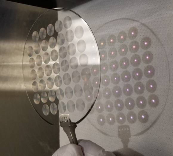
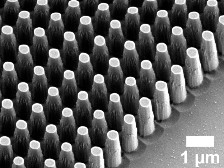
・ ハーバード大学が、全ガラス製でセンチメートルサイズの可視スペクトルメタレンズを開発。従来のチップ製造技術のリソグラフィーを用いて作製できる。
・ 同新技術は、平坦な CMOS チップとメタレンズを簡易な光学的配列により直接積み重ねる、携帯電話用のいわゆるウェハーレベルカメラの開発の可能性を拓く。将来的には、リソグラフィー技術を使用した同一メーカーによるチップとレンズの両方の製造が可能に。
・ これまでは、時間がかかる電子ビームリソグラフィーや、サブ波長構造のパターニングに充分な解像度を持たない i 線ステッパーリソグラフィ技術を使用していたため、可視光波長のセンチメートルスケールメタレンズの量産ができなかった。
・ 同メタレンズ量産では、コンピューターや携帯電話のシリコンチップの微細なラインや形状のパターニングに広く使用される、深紫外(DUV)投影リソグラフィー技術を採用。数百万個ものナノスケールの要素から成るメタレンズを、1 回の露光でチップ毎に大量に製造できる。
・ また、ナノ構造パターンをガラス表面に直接エッチングすることで、従来のメタンレンズ製造では必要だった時間のかかる蒸着プロセスを排除。初の量産可能なセンチメートルスケールの全ガラス製可視スペクトルメタレンズとなる。
・ ただし、同新メタレンズは、光の波長によって焦点位置がずれる色収差の課題があるため、大口径のアクロマティック・メタレンズの作製に取り組む。
・本研究は、米国防高等研究計画局の支援を一部受けた。本研究は、米国立科学財団(NSF)支援下
の National Nanotechnology Coordinated Infrastructure (NNCI)のメンバーである Cornell NanoScale
Science & Technology Facility および Harvard University Center for Nanoscale Systems にて一部実施された。
URL: https://www.seas.harvard.edu/news/2019/12/metalens–grows
(関連情報)
Nano Letters 掲載論文(アブストラクトのみ:全文は有料)
All-Glass, Large Metalens at Visible Wavelength Using Deep-Ultraviolet Projection Lithography
URL: https://pubs.acs.org/doi/10.1021/acs.nanolett.9b03333
<NEDO海外技術情報より>
Abstract
Abstract Image
Metalenses, planar lenses realized by placing subwavelength nanostructures that locally impart lenslike phase shifts to the incident light, are promising as a replacement for refractive optics for their ultrathin, lightweight, and tailorable characteristics, especially for applications where payload is of significant importance. However, the requirement of fabricating up to billions of subwavelength structures for centimeter-scale metalenses can constrain size-scalability and mass-production for large lenses. In this Letter, we demonstrate a centimeter-scale, all-glass metalens capable of focusing and imaging at visible wavelength, using deep-ultraviolet (DUV) projection stepper lithography. Here, we show size-scalability and potential for mass-production by fabricating 45 metalenses of 1 cm diameter on a 4 in. fused-silica wafer. The lenses show diffraction-limited focusing behavior for any homogeneously polarized incidence at visible wavelengths. The metalens’ performance is quantified by the Strehl ratio and the modulation transfer function (MTF), which are then compared with commercial refractive spherical and aspherical singlet lenses of similar size and focal length. We further explore the imaging capabilities of our metalens using a color-pixel sCMOS camera and scanning-imaging techniques, demonstrating potential applications for virtual reality (VR) devices or biological imaging techniques.
KEYWORDS:Metalens metasurface DUV lithography visible wavelength all-glass