(Printed Electronics Open Way for Electrified Tattoos and Personalized Biosensors)
2019/10/3 アメリカ合衆国・デューク大学

・ デューク大学が、紙や人間の皮膚などの繊細な表面上でも十分に機能するプリンテッド・エレクトロニクスを作製する、完全な一体造形(print-in-place)3D プリンティング技術を開発。密着性の高い、埋め込み型の電子タトゥーや、個々の患者特製のバイオセンサーを埋め込んだ包帯などに使用できる。
・ このような完全なプリンテッド・エレクトロニクスについては、長年研究されてはきたものの、作製するためには、サンプルを何度も取り出して焼結、洗浄や、蒸着したりする工程が必要で、実現はされていなかった。新技術は、そのような従来の課題を克服するもの。
・ いわゆる電子タトゥーの概念は、2000 年代後半に、当時イリノイ大学在籍で、現在はノースウェスタン大学の Louis Simpson and Kimberly Querrey 材料科学工学教授の John A. Rogers 氏により開発された。皮膚に直接、永久的に入れ墨を入れる本物のタトゥーに比べ、電子タトゥーは、フレキシブルな電子機器を含んだ、細くてフレキシブルなゴムのパッチ。
・ この薄いフィルムは皮膚に一時的なタトゥーのように張り付き、初期段階のフレキシブル・エレクトロニクスでは、心臓や脳の活動のモニタリングや筋肉を刺激したりするために作製されていた。現在では、商業化・大量生産化に向かっているが、例えば、カスタム・エレクトロニクス添加により表面に直接修正が必要な場合があるなど、うまく機能していない部分も見つかっている。
・ 3D プリンティング技術を真に有用なものにするには、オブジェクト全体をワンステップでプリント作製する必要がある。
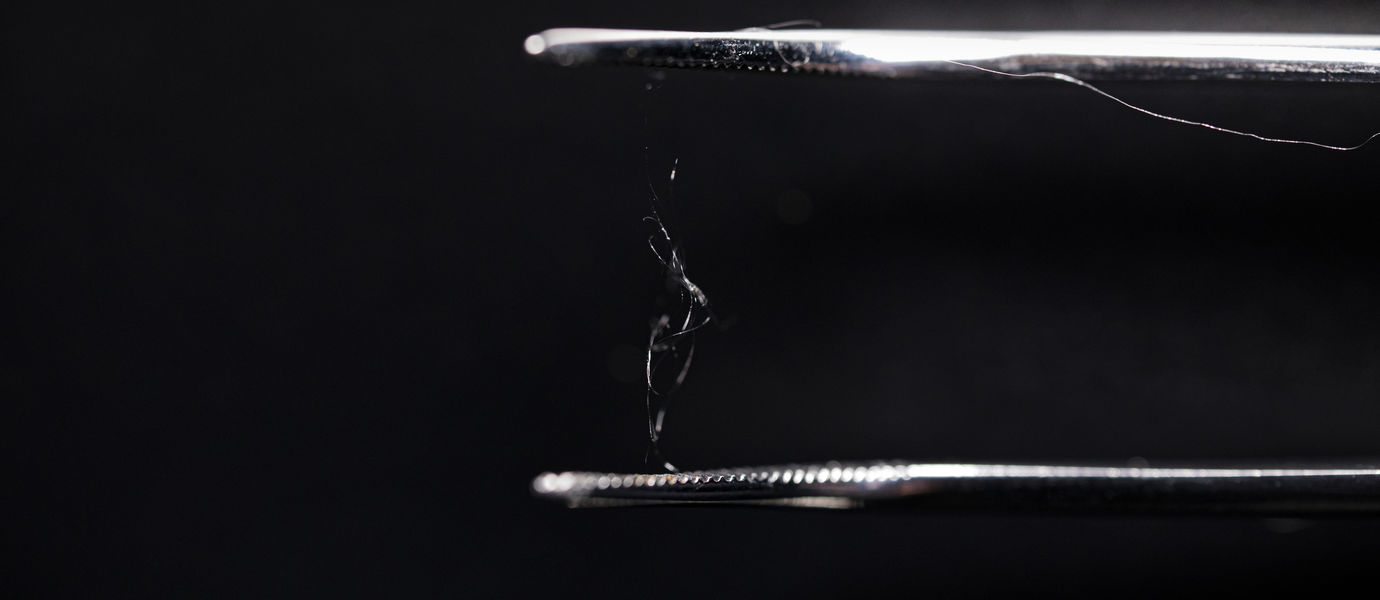
・ 本研究では、どんな構造体でも低温でエアロゾルプリンターを使用してプリントできる、銀ナノワイヤを含んだ新しいインクを開発。追加工無く導電性を維持する薄いフィルムを作製。プリント後、インクは 2 分以内で乾燥し、50%の曲げひずみを千回以上繰り返した後でも、高い電気性能を保持。
・ 本論文に添付された実証ビデオでは、小指の下部に沿って、電子的に活性な 2 本のリード線をプリントしている。リード線は、小指先端に向かって小型 LED ライトに接続。リード線に電圧をかけると、 LED ライトは点灯し、小指を曲げ伸ばしても消灯しない。
・ 本研究の二番目の論文では、導電性のインクを他の 2 つのプリント可能な構造体と組み合わせてトランジスタを作製。初めにカーボンナノチューブの半導体片をプリントし、乾燥したら、プラスチックや紙製の基板をプリンターから外さずに、数 cm の 2 つの銀ナノワイヤリード線をプリントする。・ 非導電性誘電体層には、2D 材料の六方晶窒化ホウ素で半導体片の上にプリント。その後、銀ナノワイヤリード線のゲート電極をプリントする。
・ 従来の技術では、例えば不要な材料を化学物質で洗い流したり、各層が混在しないように硬化させたり、電気的フィールドを遮る有機材料の痕跡を除去するために焼結したりと、追加工が必要であった。・ 新技術では、このような追加工は不要。材料が混在しないように各層を完全に乾燥させる必要もなく、処理する温度は従来よりも低温で可能。
・ 本技術は、ウェアラブルエレクトロニクスの大規模な大量製造技術を置き換えるものではないが、ラピッドプロトタイピング技法やワンサイズですべてがまかなえないアプリケーションなどに使用できる可能性がある。
・ 本研究は、米国防総省(DOD)の Congressionally Directed Medical Research Program (W81XWH-17- 2-0045) 、米国立衛生研究所(NIH)(1R21HL141028)および、米国立科学財団(NSF)(ECCS-1542015)より支援を受けた。
URL: https://pratt.duke.edu/about/news/print-in-place-electronics
(関連情報)
Nanoscale 掲載論文(アブストラクトのみ:全文は有料)
Silver nanowire inks for direct-write electronic tattoo applications
URL: http://dx.doi.org/10.1039/c9nr03378e
(関連情報) ACS Nano 掲載論文(アブストラクトのみ:全文は有料)
Flexible, Print-in-Place 1D–2D Thin-Film Transistors Using Aerosol Jet Printing
URL: https://pubs.acs.org/doi/10.1021/acsnano.9b04337#
<NEDO海外技術情報より>
Abstract
Room-temperature printing of conductive traces has the potential to facilitate the direct writing of electronic tattoos and other medical devices onto biological tissue, such as human skin. However, in order to achieve sufficient electrical performance, the vast majority of conductive inks require biologically harmful post-processing techniques. In addition, most printed conductive traces will degrade with bending stresses that occur from everyday movement. In this work, water-based inks consisting of high aspect ratio silver nanowires are shown to enable the printing of conductive traces at low temperatures and without harmful post-processing. Moreover, the traces produced from these inks retain high electrical performance, even while undergoing up to 50% bending strain and cyclic bending strain over a thousand bending cycles. This ink has a rapid dry time of less than 2 minutes, which is imperative for applications requiring the direct writing of electronics on sensitive surfaces. Demonstrations of conductive traces printed onto soft, nonplanar materials, including an apple and a human finger, highlight the utility of these new silver nanowire inks. These mechanically robust films are ideally suited for printing directly on biological substrates and may find potential applications in the direct-write printing of electronic tattoos and other biomedical devices.